i-SEDEX Evolves Into I
ntegrated Int'l Semiconductor Fair
Some 200 exhibitors from 10 countries participate in the exhibition
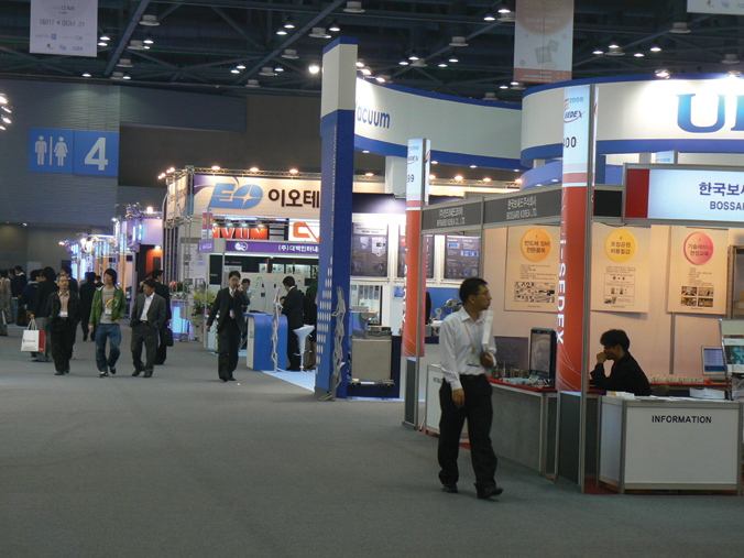
 The 10th International Semiconductor Exhibition (i-SEDEX 2008) was held at KINTEX in Goyang, north of Seoul, from Oct. 14-17 with 200 exhibitors from 10 countries participating.
I-SEDEX, the new name of SEDEX Korea, has expanded in line with the demands of internationalization. I-SEDEX, the nation's largest-scale international exhibition in the area of semiconductors and displays, held in connection with prominent domestic and foreign device companies, not only provides a stepping stone for excavating new customers by maximizing the marketing effects of the participating companies, but also enhances its value, organizers said.
The exhibition was hosted by the Ministry of Knowledge Economy and managed by the Korea Trade-Investment Promotion Agency (KOTRA), the Korea Semiconductor Industry Association (KSIA) and the Consortium of Semiconductor Advanced Research (COSAR).
In his message, Kwon Oh-hyun, KSIA chairman, said,
 "I-SEDEX marks the 10th anniversary since 1999 when the exhibition was inaugurated to publicize abroad Korea's standing as a global semiconductor powerhouse and to exchange semiconductor products and advanced technologies. The exhibition has evolved into an integrated international semiconductor fair with an annual growth rate of more than 20 percent with the active support of Korean and foreign semiconductor makers."In an effort to be on a par with globally recognized fairs, including CES and CeBIT, i-CEDEX was held simultaneously with KES 2008 and IMID 2008 (International Meeting on Information Display) starting this year, with a view of attracting more global IT and electronics industry officials from across the world. nw
A view of i-SEDEX 2008
SAMSUNG'S Smallest 2 Gigabit DDR3
Power Savings of 40 percent or More for Servers and PCs
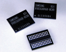
Samsung Electronics Co., Ltd., the world leader in advanced memory technology, announced today that it is sampling the industry's smallest two gigabit (Gb) DDR3 devices. By using 50 nanometer (nm) class circuit technology, the productivity of the new devices is 60 percent higher than DDR2 devices of an equivalent density. The new 2Gb DDR3-based modules, which enables use of up to 16 gigabytes (GB) of RIMMs (registered in-line memory modules), will consume only 40 percent of the power of 1Gb DDR3 memory modules.
"We have focused on maximizing density alternatives and power savings to make our 2Gb DDR3 solution as flexible as possible for designers,"said Jim Elliott, Vice President of Memory, Samsung Semiconductor, Inc.
The new device's small form factor enables the use of up to 8GB of memory chips for RIMMs (registered in-line memory modules), as well as 4GBs for SODIMMs (small outline dual in-line memory modules) and UDIMMs (unregistered in-line memory modules), without the need for stacking components. In addition, 2Gb DDR3 RIMMs can be designed to 16GBs by applying dual-die packages.
The monolithic 2Gb chips are energy-efficient solutions for high-density, high-performance memory applications. The 2Gb chip replaces dual-chip solutions having two 1Gb memory devices, and reduces power consumption by at least 40 percent, which is critical in server applications as well as next-generation desktops and notebooks. The 2Gb device supports a data rate of up to 1.3 gigabits per second (Gbps) at 1.5 or 1.35 volts, up to 1.6-times faster than an 800Mbps 1Gb-based dual-die package. In addition, the reduced number of DDR3 chips lowers heat emissions.
The 50nm-class process being used to manufacture Samsung's 2Gb DDR3 is expected to become Samsung's primary DRAM process technology next year. Mass production is slated to begin later this year.
Samsung's record of DRAM innovation stretches from the introduction of 150nm-class DRAM technology in 2000, to volume production of 1Gb DDR2 using 50nm-class process technology last April. nw
3Fl, 292-47, Shindang 6-dong, Chung-gu, Seoul, Korea 100-456
Tel : 82-2-2235-6114 / Fax : 82-2-2235-0799