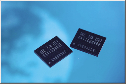
Samsung's 50nm-Class, 1Gb
DDR2 Memory Validated to
Support Intel-based Platforms
The industry's most advanced DRAM developed in October 2006
 Samsung Electronics Co., Ltd., the world leader in advanced memory technology, announced on July 19 that its 50 nanometer (nm)-class DDR2 (double data rate) DRAM - the industry's most advanced DRAM (dynamic random access memory) - has been certified by Intel Corporation to work with Intel's existing and next-generation chipsets at speeds of 800 megabits per second (Mbps).
Samsung's 1Gb DDR2 DRAM that uses the 50nm-class process technology was developed in October 2006. No other company has yet developed similar process technology for DDR2.
Processing 1Gb DDR2 DRAMs in the 50nm range doubles the productivity of a 1Gb DDR2 DRAM fabricated using 80nm process technology, while improving production efficiency by 50% over DRAM produced using the 60nm fabrication process.
As the use of Windows Vista-based PCs is expected to grow significantly in the enterprise markets during the second half of this year, demand for higher-capacity main memory should increase proportionately.
The market is expected to shift from 512Mb DRAM to 1Gb DRAM memory and set manufacturers will transition from DDR2 to DDR3 beginning in late 2007.
Samsung's 50nm-class DRAM processing technology, now validated by Intel, will be used in mass producing DDR2 beginning the first half of next year, as well as other next-generation DRAM memory, including DDR3, GDDR4 and GDDR5, plus the latest mobile DRAM.
Intel validated Samsung's 60nm-class chip design technology last March. Samsung was the first to begin mass production at the 60nm-class earlier this year and will be the first to start mass producing in the 50nm range next year. Other companies are still employing the 60nm, 70nm or 80nm design rule. nw
3Fl, 292-47, Shindang 6-dong, Chung-gu, Seoul, Korea 100-456
Tel : 82-2-2235-6114 / Fax : 82-2-2235-0799