Samsung Declares Global
'Flashtopia'
Announces the first prototype of the next-generation of memory
 Samsung Electronics Co., Ltd. announced major component technology advancements including the 40-nanometer (nm) 32-Gigabit (Gb) NAND flash, the first prototype of the next-generation of memory -PRAM (Phase change Random Access Memory), and a new System-on-Chip controller for the soon-to-be-released Hybrid Hard Disk Drive.
"The phenomenal shift in the popularity of digital products that we are experiencing today is rooted in the virtually non-stop string of advances being seen in semiconductor technology,"said Dr. Hwang Chang-kyu, at the sixth annual press conference held at the Shilla Hotel in downtown Seoul, Korea. "Anchored by major developments in NAND flash memory as today's key storage medium, digital technologies are rapidly converging to create a massive wealth of new capabilities and further convenience, representing the beginning of a new era -- Flashtopia."Samsung anticipates flash technology to continue to enable a new world of digital performance where consumers can affordably take whatever amounts of entertainment and informational data they want to wherever they want to go. As the world moves toward greater globalization and more universal dissemination of
 information, Dr. Hwang said providing the convenience of added portability through a broad diversity of flash-driven mobile applications will bring about a new utopia of storage-based freedom, which Samsung is referring to as Flashtopia.
Highlighting the conference, Samsung introduced the world's first NAND flash memory incorporating a revolutionary new 'Charge Trap Flash'(CTF) technology.
The new CTF technology, Dr. Hwang said, will extend the life span of NAND flash well beyond 40-nm level of manufacturing process technology, allowing for greater product miniaturization and greater economies of scale in the production of consumer electronics.
Following the 'New Memory Growth Theory' which Samsung's Dr. Hwang first predicted in a keynote at ISSCC in 2002, the 40nm CTF-based NAND flash memory represents a seventh generation of the New Memory Growth Theory, which has memory density doubling every twelve months. Samsung expects CTF-based NAND eventually to be refined down to 20nm at the 256 Gigabit-level.
 NAND flash has been the data storage device in virtually all digital cameras, USB drives and MP3players, as well as most multimedia handsets and smart phones. This year, NAND flash also is entering the PC computing environment. Samsung launched the first solid-state-disk (SSD) notebooks, called SENS Q3-SSD and SENS Q1-SSD in June. Their higher performance, lighter weight and enhanced storage reliability are key factors attracting mobile developers to NAND flash.
At the conference, Samsung also announced development of a System - on-Chip controller for the Hybrid drive. The new SoC represents the diversity of advanced core technologies Samsung provides.
The tremendous advancements in storage technology have spurred previously unthinkable levels of growth with much more to come. What used to be a 200-million-units-a-year PC-driven industry has become a one-billion-units-per-year mobile-driven industry. As a pivotal market-driving force, flash storage is evolving further within the digital consumer space and in professional fields such as biotechnology.
 A major advantage in PRAM is its extremely fast performance. Because PRAM can rewrite data without having to first erase data previously accumulated, it is effectively 30-times faster than conventional flash memory. Incredibly durable, PRAM is also expected to have at least 10-times the life span of flash memory.
PRAM will be a highly competitive choice over NOR flash, available beginning sometime in 2008. Samsung designed the cell size of its PRAM to be only half the size of NOR flash. Moreover, it requires 20 percent fewer process steps to produce than those used in the manufacturing of NOR flash memory.
Samsung's new PRAM was developed by adopting the use of vertical diodes with the three-dimensional transistor structure that it now uses to produce DRAM. The new PRAM has the smallest 0.0467um2 cell size of any working memory that is free of inter-cell noise, allowing virtually unlimited scalability.
Adoption of PRAM is expected to be especially popular in the future designs of multi-function handsets and for other mobile applications, where faster speeds translate into immediately noticeable boosts in performance. High-density versions will be produced first, starting with 512 Mb.
In the hybrid drive, Samsung's new SoC supports up to 4Gb flash memory as a data buffer. It maximizes the 'disk spindle down'mode and reduces power consumption levels up to 80 percent compared with the conventional HDD (hard disk drive) and improves drive reliability. It also supports the initial boot from the OneNANDTM, reducing the overall boot time by over 10 seconds.
Samsung's SoC solution for the hybrid drive incorporates a high-speed serial ATA interface with native command queuing, an HDD controller, a SDRAM controller, a OneNAND controller, and Agere read channel into a single piece of silicon. The SoC solution also includes a dual CPU core (ARM7 and ARM9) embedded to enable independent operation of the memory, HDD, and motor.
The hybrid drive solutions Samsung developed are collaborated efforts of each business division: Memory, System LSI and Storage.
Samsung plans to mass produce the SoC in November. nw
Dr. Hwang Chang-kyu, Samsung Electronics semiconductor president, announces the 40-nanometer (nm) 32-Gigabit (Gb) NAND flash and the first prototype of the next-generation of memory at the sixth annual press conference held at the Shilla Hotel in downtown Seoul.
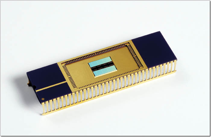
Samsung Electronics'512Mb PRAM
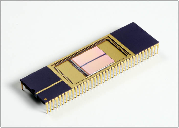
32G NAND flash, produced by Samsung Electronics
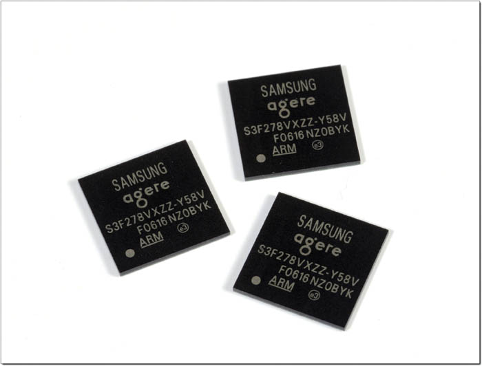
Samsung's Hybrid HDD SOC
3Fl, 292-47, Shindang 6-dong, Chung-gu, Seoul, Korea 100-456
Tel : 82-2-2235-6114 / Fax : 82-2-2235-0799