Samsung Electronics to Build Memory
Chip Fabrication Center in U.S.
Launches second investment strategy for Hwaseong plant
 Samsung Electronics plans to build an additional semiconductor plant in the United States, Hwang Chang-gyu, president of the company's semiconductor business, said.
Samsung Electronics President Hwang said on September 28 his company was considering constructing an additional semiconductor factory in the Unites States with excellent manpower and a big market after studying several candidate countries on the plan to build another overseas semiconductor fabrication plant. He made the remark in a meeting with reporters during an opening ceremony for the SEDEX Korea 2005.
"Details, (including the investment size), will be announced in an appropriate time,"Hwang said. He added that now is not the right time for his company to make an official announcement regarding the plan, but external and internal demand has been rising and seven years have already passed after the Austin factory was established. The U.S. plant, which was opened in 1998, has a DRAM fabrication line.
Samsung Electronics plans to build a 300-mm wafer memory fabrication center, company officials said, adding that the site of the projected plant, to be built with an investment of $3 billion is mostly likely to be Austin, Minn. Other U.S. states, including Arizona and Texas, have offered incentives like infrastructure support to Samsung to attract the projected semiconductor factory.
The existing Austin DRAM fabrication plant is one of Korea's overseas investment success stories because the factory, established with an employment of 1,000-plus local people in the early 1998, made a strong showing with sales worth $700 million and ordinary profits worth $160 million the following year.
Investment Strategy for Hwaseong Plant
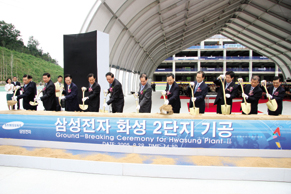
Samsung Electronics held a ground-breaking ceremony to kick off the company's second round of investments in its Hwaseong semiconductor plant on September 28. This activity marks the next step in the company's seven-year investment plan for the site. Hwaseong's second phase will be located on 230-acres / 960K-㎡ / 290K-pyong that is slated to house one R&D facility and eight fabrication lines by 2012, calling for an estimated capital expenditure (CapEx) of $33 billion.
"Breaking away from conventional concepts welcomes previously unsought of possibilities that benefit consumers with new conveniences and luxuries" Samsung President Hwang said. "By successfully executing leading-edge R&D and manufacturing technologies, we are driving the adoption of innovative semiconductor technology solutions in the marketplace."Samsung's Next-generation R&D line (NRD line) is scheduled to begin operations in May 2006. The NRD line will be a double tiered structure clean room with adjoining office space for research and development of next-generation technologies including nano and process technology, and other materials for both memory and system LSI semiconductors. The company's total investment for the second 300mm R&D line is expected to be approximately $860 million.
The NRD line is the newest addition to Samsung's five existing R&D dedicated lines where future advancements in memory and logic technologies such as PRAM, FRAM, DRAM, Flash memory, and CMOS image sensors are currently taking place. Samsung expects its total R&D workforce to add 5,000 more engineers by 2012.
Long-Term Dedication to IT Innovations
Samsung's main semiconductor fabrication site, Giheung, was established in 1983. After installing a total of fifteen fabrication and R&D lines in Giheung, an expansion was initiated in nearby Hwaseong, giving the entire site the name Giheung-Hwaseong. When completed in 2012, Samsung's Giheung-Hwaseong complex will be the world's largest semiconductor fabrication facility.
The long-term investment plan reflects Samsung's strong commitment to supporting leading-edge technologies that will create new markets and applications. This investment plan will be fine-tuned periodically through short and long-term market reviews.
As part of the second-phase at the Hwaseong complex, the first fabrication line, line no.15, is currently under construction with plans to finalize the outer shell by the first half of 2006. Out of the eight new fabrication lines, Samsung expects four to be designed for capacities higher than conventional lines with the possibility of a 300mm or larger wafer-unit. The entire expansion project is expected to bring about 14,000 new jobs to the Korean economy.
The Hwaseong plant was first established in 2000. Phase-one housed five fabrication lines and one R&D line, R2 line, on a total area of 150-acres/ 630,000-㎡/ 190,000-pyong. After opening its first 300mm-fab MPS line in 2001, Samsung experienced a steep growth in global memory semiconductor market share from 18 percent in 2001 to 25 percent in 2002.
Samsung's timely investments are based on careful analysis and market sensing, enabling the company to meet new demands ahead of the competition. Such aggressive but carefully planned investments has built the backbone of the company's highly profitable performance during the past decade. nw
A project to make Samsung Electronics'second round of investments in its Hwaseong semiconductor plant breaks ground on Sept. 28.
3Fl, 292-47, Shindang 6-dong, Chung-gu, Seoul, Korea 100-456
Tel : 82-2-2235-6114 / Fax : 82-2-2235-0799